

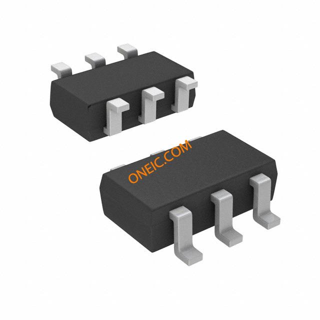
点击放大查看
SI3552DV-T1-GE3
| Manufacturer | |
| Description | Trans MOSFET N/P-CH 30V 2.5A/1.8A 6-Pin TSOP T/R N+P-FET 2/1,2A30V TSOP-6 MOSFET N/P-CH D-S 30V 6-TSOP MOSFET 30V 2.5/1.8A 1.15W 105/200mohm @ 10V |
| Category |
对参数有疑问?问 AI 助手
Business
| MOQ | 3000 | Unit Pack | 3000 |
| Other Names | SI3552DV-T1-GE3CT | Part # Aliases | SI3552DV-GE3 |
| Product Category | MOSFET | Standard Package | Tape & Reel |
| Standard Package Name | TSOP | ||
Compliance
| RoHS | Lead free / RoHS Compliant | EU RoHS | Compliant |
| Rad Hardened | No | Leadfree Defin | RoHS-conform |
Electrical
| FET Type | N and P-Channel | Vgs (Max) | ±20 V |
| FET Feature | Logic Level Gate | Power - Max | 1.15W |
| Power - Rated | 1.15 W | Fall Time (Typ) | 5@N Channel|7@P Channel ns |
| Transistor Type | N and P-Channel | Delay to 1st Tap | 13@N Channel|12@P Channel ns |
| Number of Elements | 2 | Vgs(th) (Max) @ Id | 1V @ 250µA |
| Voltage - Breakdown | 30 V | Rds On (Max) @ Id, Vgs | 105@10V@N Channel|200@10V@P Channel mOhm |
| Power Dissipation (Max) | 1150 | Propagation Delay (Max) | 9@N Channel|12@P Channel ns |
| Vce(on) (Max) @ Vge, Ic | +/- 30 V | Power (Watts) - Per Port | 1.15W |
| On-State Resistance (Max) | 105@10V@N Channel|200@10V@P Channel | Voltage - Supply (Vcc/Vdd) | 30V |
| Gate Charge (Qg) (Max) @ Vgs | 3.2nC @ 5V | Switch Time (Ton, Toff) (Max) | 7@N Channel|8@P Channel ns |
| Drain to Source Voltage (Vdss) | 30V | Current - Peak Pulse (10/1000us) | 2.5@N Channel|1.8@P Channel A |
| Voltage - Gate Trigger (Vgt) (Max) | +/- 20 V | Current - Drain (Idss) @ Vds (Vgs=0) | 2A |
| Current - Continuous Drain (Id) @ 25degC | 2.5A, 1.8A | ||
Mechanical
| Width | 1.65 | Packaging | Tape and Reel |
| Lead Style | Gull-wing | Mounting Type | Surface Mount |
| Mounting Style | SMD/SMT | Package / Case | 6TSOP |
| Package Cooled | TSOP | Length - Overall | 3.05 |
| Package Quantity | TSOP | Number of Positions | 6 |
| Shell Size - Insert | 1(Max) | Supplier Device Package | 6-TSOP |
Product Info
| Type | Power MOSFET | Polarity | N+P CHANN |
| Matchcode | SI3552DV | Channel Type | N|P |
| Configuration | Dual | Standard Leadtime | 14 weeks |
| Printed Circuit Board | 6 | ||
Environmental
| Operating Temperature | -55 to 150 °C | ||